Skip to main content
友嘉科技股份有限公司
UNION OPTRONICS CORP.
Switch Language
English
繁中
简中
Home
Products and Services
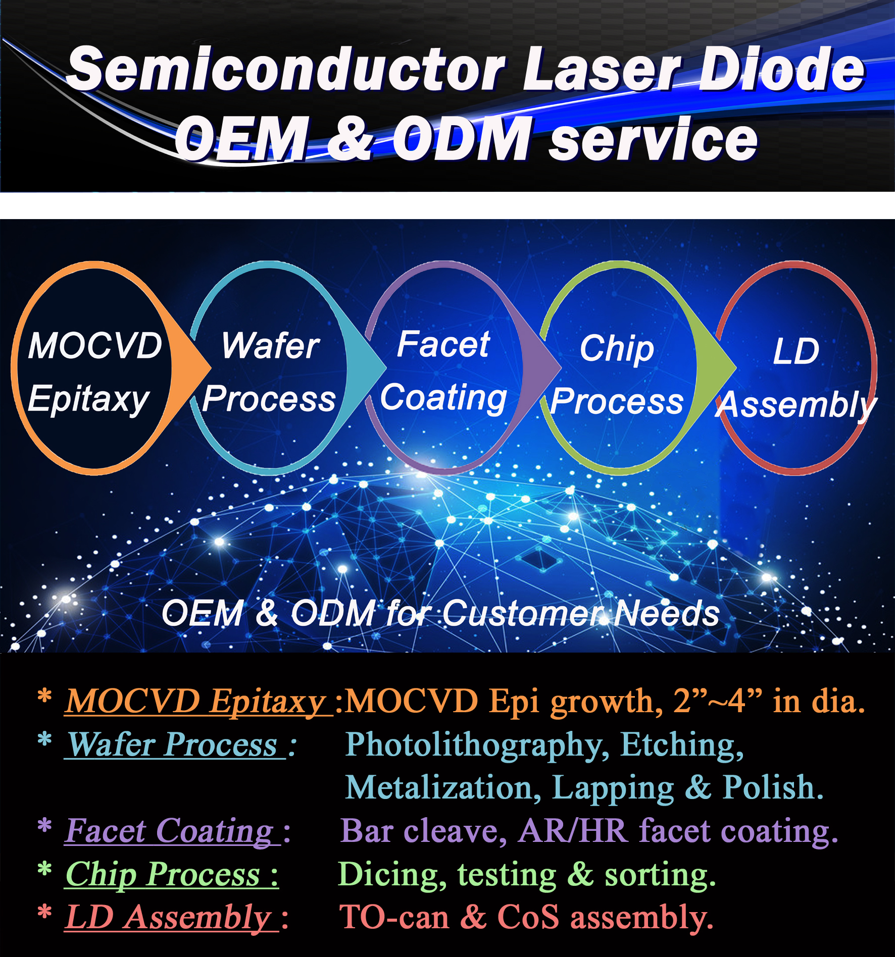
Semiconductor Laser Diodes
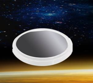
Epi wafers
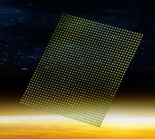
Laser Diode bare Chip & V-facet PD Chip
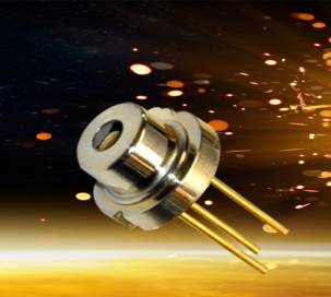
Packaged LDs
LD(TO-can)
CoS & Reflector
SMD
OEM & ODM service
About UOC
Our Profile
Quality Policy
Environmental Management
Environmental Management & Certification
Restriction of Hazardous Substances (RoHS)(RoHS 3.0)
Conflict Minerals Policy Declaration
Our Certificate
Company Info.
What's New
Exhibition
Contact UOC
Location
Inquiry
Satisfaction Survey
訪客登記
訪客登記建立
Breadcrumb
Home
OEM & ODM service
Semiconductor Laser Diodes
EPI Wafer
LD Chips
Package LDs
OEM&ODM